PCB and Chip Sample Preparation
A comprehensive guide to preparing printed circuit boards (PCBs) and semiconductor chips for metallographic analysis, with emphasis on controlled removal techniques and precision preparation methods essential for electronics failure analysis and quality control.
Table of Contents
Introduction
The preparation of printed circuit boards (PCBs) and semiconductor chips for metallographic analysis presents unique challenges that require specialized techniques and equipment. Unlike traditional metallographic samples, PCBs and chips consist of multiple layers of different materials—copper traces, solder, epoxy substrates, silicon, and various protective coatings—each with different mechanical properties and removal rates.
Successful preparation of these samples requires precision, patience, and the right equipment. The goal is to reveal cross-sections that show the true structure of interconnects, solder joints, via structures, and layer interfaces without introducing artifacts such as delamination,smearing, or relief between different materials.
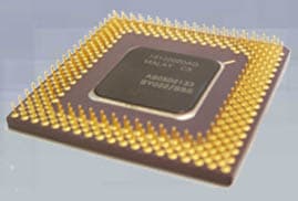
Computer chip cross-section showing multi-layer structure. Proper preparation reveals interconnects, via structures, and layer interfaces without artifacts. This demonstrates the precision required for electronics sample preparation.
Key Consideration: PCB and chip preparation is fundamentally different from traditional metallography. The multi-material nature, delicate structures, and need for precise depth control make controlled removal techniques essential for successful analysis.
Growing Demand in Electronics
The explosion of artificial intelligence (AI) and machine learning applications has dramatically increased the demand for PCB and chip analysis. AI chips, GPUs, and specialized processors require rigorous quality control, failure analysis, and process validation. This has led to a massive increase in metallographic work on electronic components.
Why the Demand is Growing
- AI Chip Development: New AI processors require validation of complex multi-layer structures, interconnects, and thermal management features
- Failure Analysis: As devices become more complex, understanding failure modes requires precise cross-sectional analysis
- Quality Control: Manufacturing processes must be validated to ensure reliability in critical applications
- Process Development: New manufacturing techniques require metallographic validation
- Reverse Engineering: Competitive analysis and intellectual property verification
- Reliability Testing: Understanding degradation mechanisms in electronic components
This increased demand has made expertise in PCB and chip preparation more valuable than ever. Laboratories specializing in electronics analysis are seeing unprecedented workloads, and the need for efficient, reliable preparation methods has never been greater.
Unique Challenges in PCB and Chip Preparation
Preparing PCBs and chips for metallographic analysis presents several unique challenges that distinguish this work from traditional metallography:
Multi-Material Systems
PCBs and chips contain multiple materials with vastly different properties:
- Copper: Soft, ductile, prone to smearing
- Solder: Very soft, low melting point, can flow during preparation
- Epoxy/FR4: Brittle, can delaminate, different removal rate than metals
- Silicon: Hard, brittle, can chip or crack
- Protective Coatings: Often very thin, easily removed or damaged
- Dielectric Layers: Soft, can be easily scratched or deformed, requiring careful polishing to avoid artifacts
Delicate Structures
Modern electronics contain extremely fine features:
- PCB trace widths from hundreds of micrometers down to roughly 25-50 μm on HDI boards; on-die interconnects inside the chip itself reach the nanometer scale
- Via diameters of 50-100 μm or smaller
- Copper layers from about 17 μm (½ oz) to 70 μm (2 oz), with dielectric layers typically 50-200 μm
- Solder joints with critical dimensions requiring precise preparation
- Bond wires and interconnects
Precision Requirements
Many applications require precise depth control:
- Targeting specific layers or features
- Removing exact amounts of material (metered removal)
- Preparing samples for specific analysis techniques (SEM, FIB, TEM)
- Maintaining planarity across the entire sample to avoid relief
Critical Point: These challenges make traditional metallographic techniques insufficient. Controlled removal systems are not just beneficial—they are often essential for successful PCB and chip preparation.
Sectioning PCBs and Chips
Sectioning is the first critical step in PCB and chip preparation. The goal is to cut through the sample to reveal the cross-section of interest while minimizing damage to delicate structures.
Thin precision cutting blades (0.3-0.5 mm) minimize kerf loss and reduce damage to delicate PCB and chip structures. Precision wafering techniques are ideal for electronics.
Sectioning Considerations
- Light Load: Use a precision saw with light loads (typically 100-500 g for silicon and package cross-sections; 30-80 g for delicate multilayer ceramic capacitors) to minimize heat generation and mechanical damage. Resin-bond diamond wafering blades on silicon typically run 2,500-5,000 RPM—control damage with load and blade selection rather than feed force
- Thin Blades: Use thin diamond blades or abrasive blades (0.3-0.5 mm) to minimize kerf loss and reduce damage
- Coolant: Adequate coolant is essential to prevent overheating, which can damage solder joints and cause delamination
- Orientation: Plan the cut direction to reveal the features of interest (traces, vias, solder joints)
- Support: Support fragile samples to prevent cracking during cutting
Sectioning Procedure
- Identify the area of interest and mark the cutting plane
- Secure the sample in the cutting fixture
- Use a thin, fine-grit abrasive blade or diamond blade
- Cut with a light, steady load and let the blade run at its rated speed
- Use continuous coolant flow
- Allow the blade to do the cutting—avoid forcing
- After cutting, clean the sample thoroughly to remove cutting debris
Example Products: Precision Sectioning EquipmentPrecision sectioning saws with variable speed control for delicate electronics
For purchasing options and product specifications, see commercial supplier website.
Mounting Techniques
Mounting provides edge retention and protects delicate structures during preparation. For PCBs and chips, mounting is critical because the multi-layer structures are prone to delaminationand edge damage.
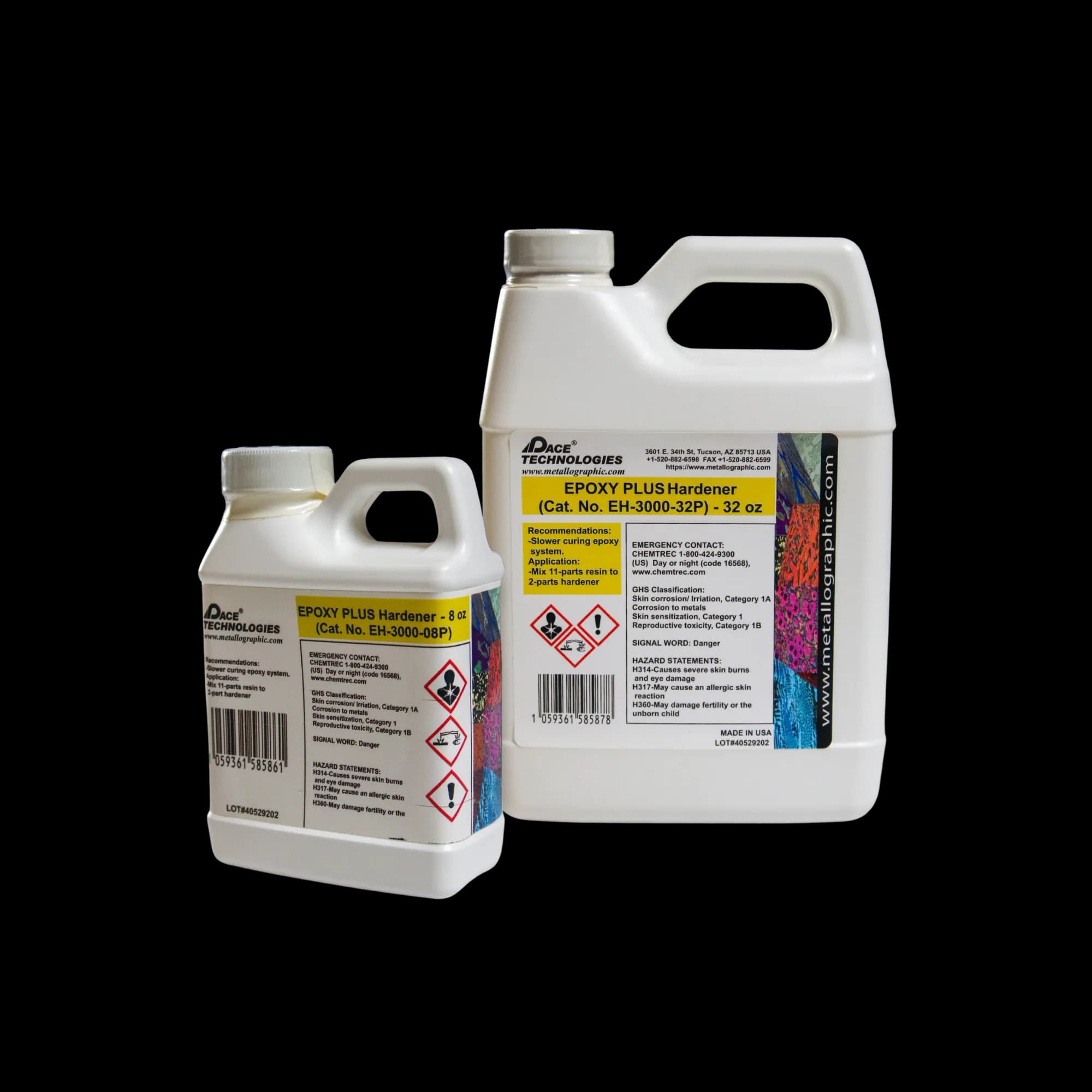
Epoxy castable mounting resin provides excellent edge retention for delicate PCB structures.

Mounting equipment and accessories for both compression and castable mounting.
Mounting Material Selection
Epoxy Resin: Preferred for PCBs and chips because:
- Excellent edge retention
- Low shrinkage minimizes stress on delicate structures
- Transparent options allow viewing of sample orientation
- Good adhesion to various materials
- Can be used at room temperature (castable) or elevated temperature (compression)
Mounting Procedure
- Clean the sample thoroughly to remove cutting fluid and debris
- If using castable epoxy, mix according to manufacturer's instructions
- Place sample in mounting cup with the cut surface (the surface to be prepared) facing down against the bottom of the cup
- Pour epoxy carefully to avoid bubbles
- Allow to cure completely (typically 6-12 hours for a slow-cure, low-shrinkage epoxy)
- Avoid compression mounting for solder joints and other heat- or pressure-sensitive packages—the heat and pressure can damage the sample. Reserve it for robust samples only, at reduced pressure and temperature
Tip: For samples with very delicate structures, consider using vacuum impregnation to ensure complete penetration of mounting material into any voids or cracks.
Grinding and Initial Preparation
Grinding removes sectioning damage and prepares the surface for controlled removal polishing. For PCBs and chips, grinding must be done carefully to avoid delamination and maintain the integrity of multi-layer structures.
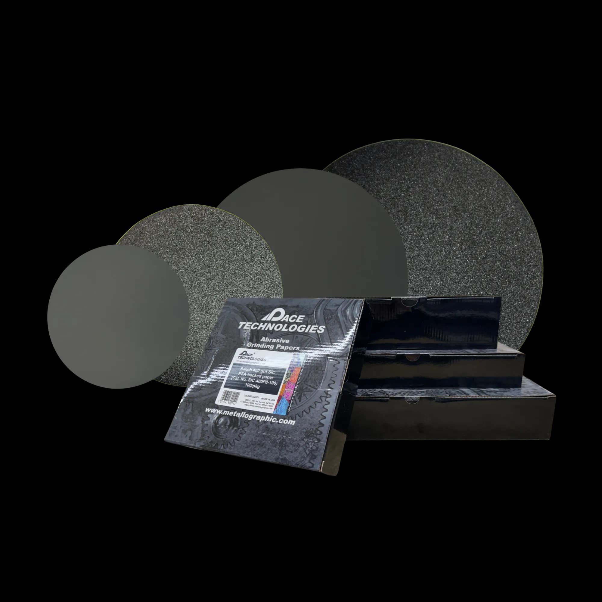
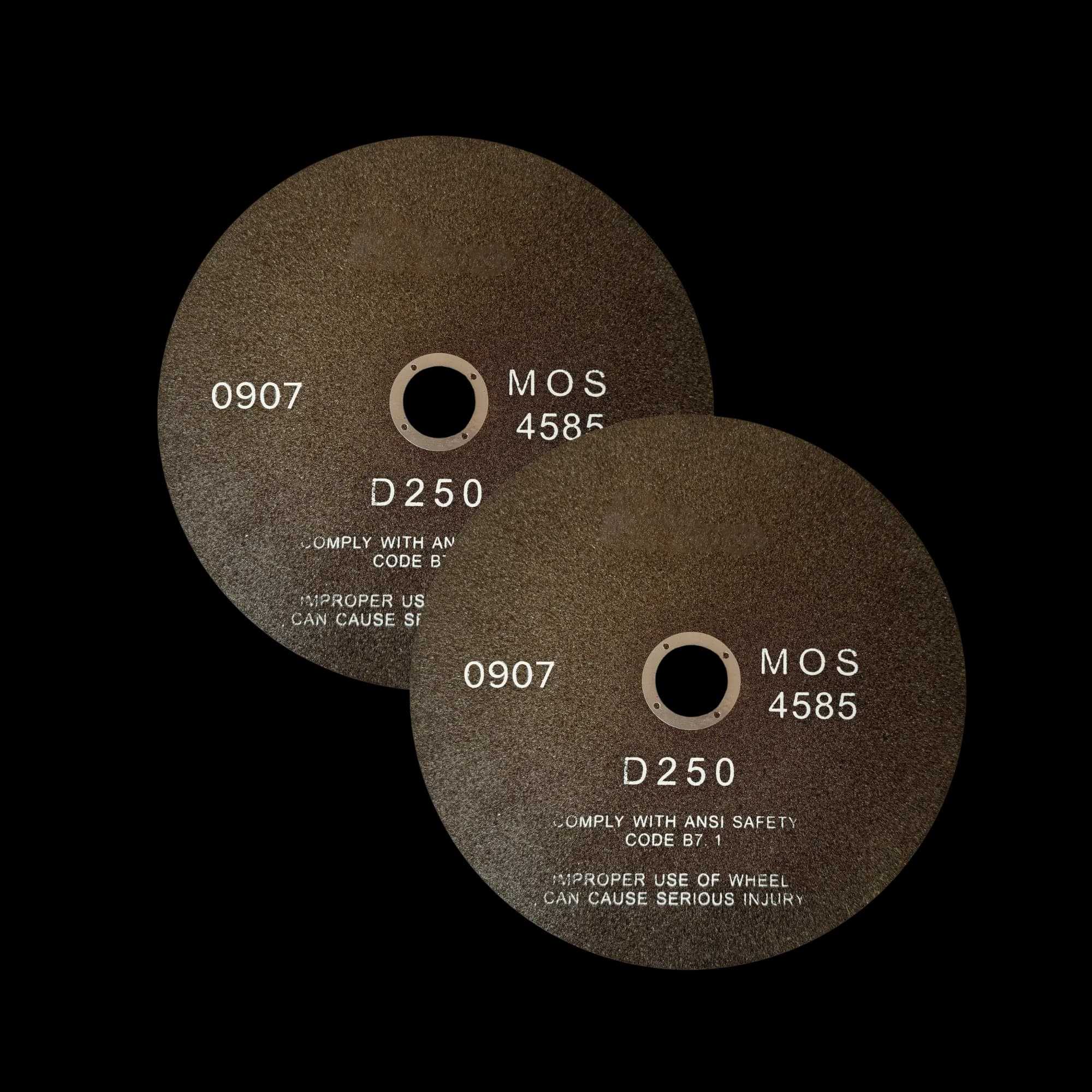
Silicon carbide (SiC) abrasive grinding papers in fine grit sizes (400, 600, 800, 1200) for progressive grinding. Use light pressure to avoid delamination of delicate PCB layers.
Grinding Sequence
Use a progressive grinding sequence with fine grits:
- 400 grit: Remove sectioning damage (30-60 seconds, light pressure)
- 600 grit: Remove previous scratches (30-60 seconds)
- 800 grit: Further refinement (30-60 seconds)
- 1200 grit: Final grinding step (30-60 seconds)
Grinding Best Practices
- Light Pressure: Use minimal pressure to avoid delamination
- Water Lubrication: Continuous water flow prevents overheating
- Rotation: Rotate sample 90° between grits to ensure complete scratch removal
- Time Control: Don't over-grind—just remove previous scratches
- Inspection: Check frequently under low magnification to monitor progress
Warning: Excessive grinding time or pressure can cause delamination, especially at layer interfaces. If you see signs of delamination, reduce pressure and grinding time.
Example Products: Silicon Carbide Grinding PapersFine grit SiC papers for progressive grinding of delicate electronics
For purchasing options and product specifications, see commercial supplier website.
Controlled Removal - The Critical Technique
Controlled removal, also known as metered removal, is the most important technique for PCB and chip preparation. This method allows for precise material removal in micrometer-level increments, making it essential for applications requiring exact depth control or targeting specific features.
Why Controlled Removal is Essential
Traditional polishing methods remove material at variable rates depending on the material being polished. In multi-material systems like PCBs and chips, this creates several problems:
- Relief: Softer materials (copper, solder) polish faster than harder materials (silicon, epoxy), creating height differences
- Over-removal: Without precise control, you may remove too much material and lose the feature of interest
- Under-removal: You may not remove enough material to reach the target depth or feature
- Inconsistency: Manual polishing produces variable results, making it difficult to prepare multiple samples to the same depth
Controlled removal systems solve these problems by providing real-time feedback and precise control over material removal.
How Controlled Removal Works
Controlled removal systems use precision measurement and feedback to remove material in exact increments. The system monitors removal in real-time with micrometer-level resolution, allowing operators to:
- Remove precise amounts of material (e.g., 5 μm, 10 μm, 50 μm)
- Target specific layers or features
- Maintain consistent removal rates across the sample
- Prepare multiple samples to the same depth
- Achieve planarity across multi-material systems
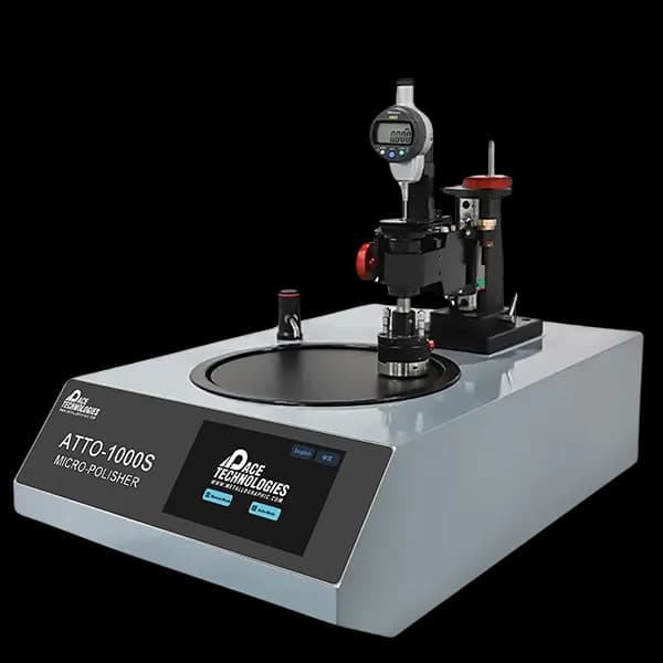
A controlled removal polisher provides the micrometer-level precision essential for PCB and chip preparation. Real-time monitoring and feedback ensure precise material removal to target specific features or depths.
Key Features of Controlled Removal Systems
- Micrometer-Adjustable Control: Pitch and roll control for exacting results
- Real-Time Monitoring: Sub-micron (typically ~0.2 μm) resolution removal monitoring
- Precise Load Control: Sample load control (typically 0-300 grams)
- Variable Speed: Optimal material removal rates for different materials
- Touchscreen Interface: Easy operation and parameter adjustment
- Planarity Control: Maintains flatness across multi-material samples
Controlled Removal Procedure
- Initial Setup:
- Mount sample securely in holder
- Set initial load (typically 50-150 grams for PCBs)
- Select appropriate polishing pad and compound
- Set polishing speed to a slow, controlled rate per the manufacturer's recommendations
- Calibration:
- Calibrate the system according to manufacturer's instructions
- Verify removal rate with a test sample if needed
- Polishing:
- Start with coarse diamond (9 μm or 6 μm) for initial material removal
- Monitor removal in real-time on the display
- Adjust parameters as needed to maintain desired removal rate
- Continue until target depth is reached or sectioning damage is removed
- Progressive Refinement:
- Move to finer diamond sizes (3 μm, 1 μm) for surface refinement
- Continue monitoring removal to ensure consistent progress
- Adjust load and speed for optimal results
- Final Polish:
- Use 0.05 μm colloidal silica for final polish
- Minimal removal at this stage—focus on surface finish
- Verify final depth and surface quality
Applications Requiring Controlled Removal
- IC Flip Chip Preparation: Precise removal to reveal bump structures and interfaces
- Via Analysis: Targeting specific via layers or depths
- Layer Thickness Measurement: Removing exact amounts to measure layer thicknesses
- Failure Analysis: Preparing samples to reveal failure sites at specific depths
- SEM/FIB Preparation: Preparing samples for electron microscopy at precise depths
- Multi-Sample Consistency: Preparing multiple samples to the same depth for comparison
- Planarity Requirements: Maintaining flatness across multi-material systems
Best Practice: For critical applications, document all parameters (load, speed, diamond size, removal rate) so procedures can be repeated consistently.
Polishing Techniques
After controlled removal, final polishing prepares the surface for high-magnification analysis. The goal is to achieve a mirror-like finish without introducing artifacts or removing too much material.
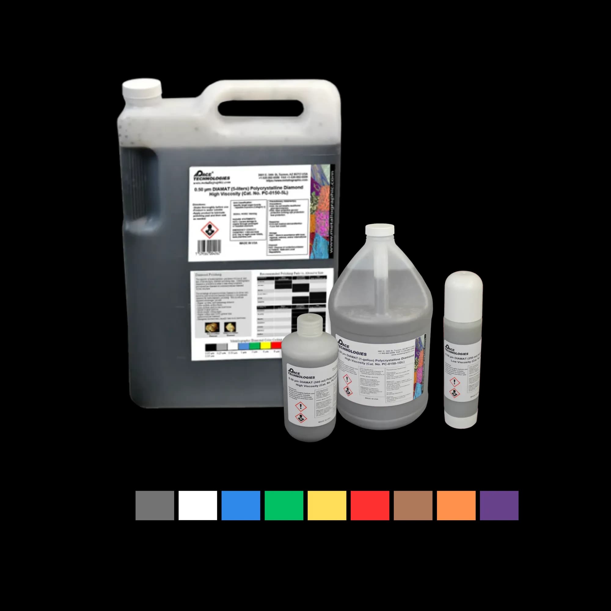
Diamond polishing compounds in various particle sizes for removing grinding scratches.
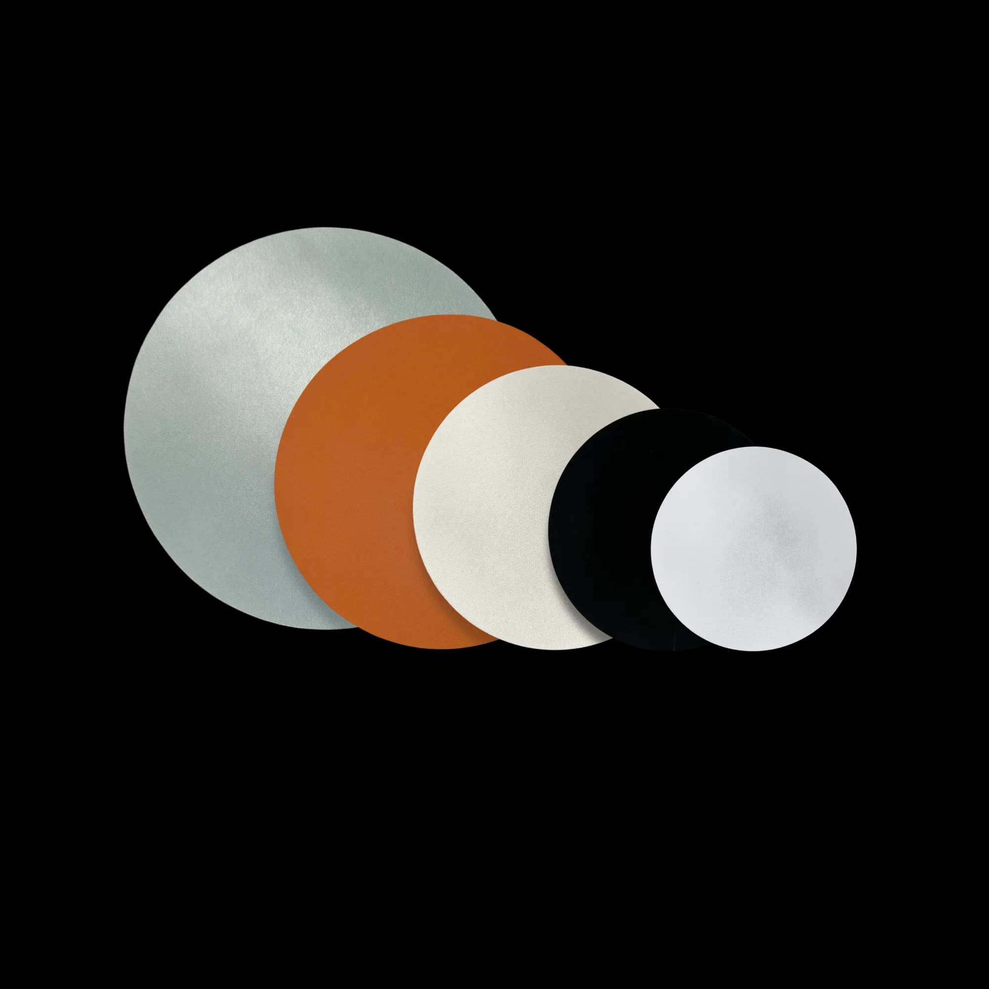
Various polishing pads and cloths for different polishing stages.
Diamond Polishing Sequence
If not using controlled removal for all steps, use this sequence:
- 9 μm diamond: 3-5 minutes on a hard, non-napped cloth (e.g., silk or woven nylon)
- 3 μm diamond: 3-5 minutes on medium-hard cloth
- 1 μm diamond: 2-3 minutes on soft cloth
Final Polishing
Final polish with colloidal silica:
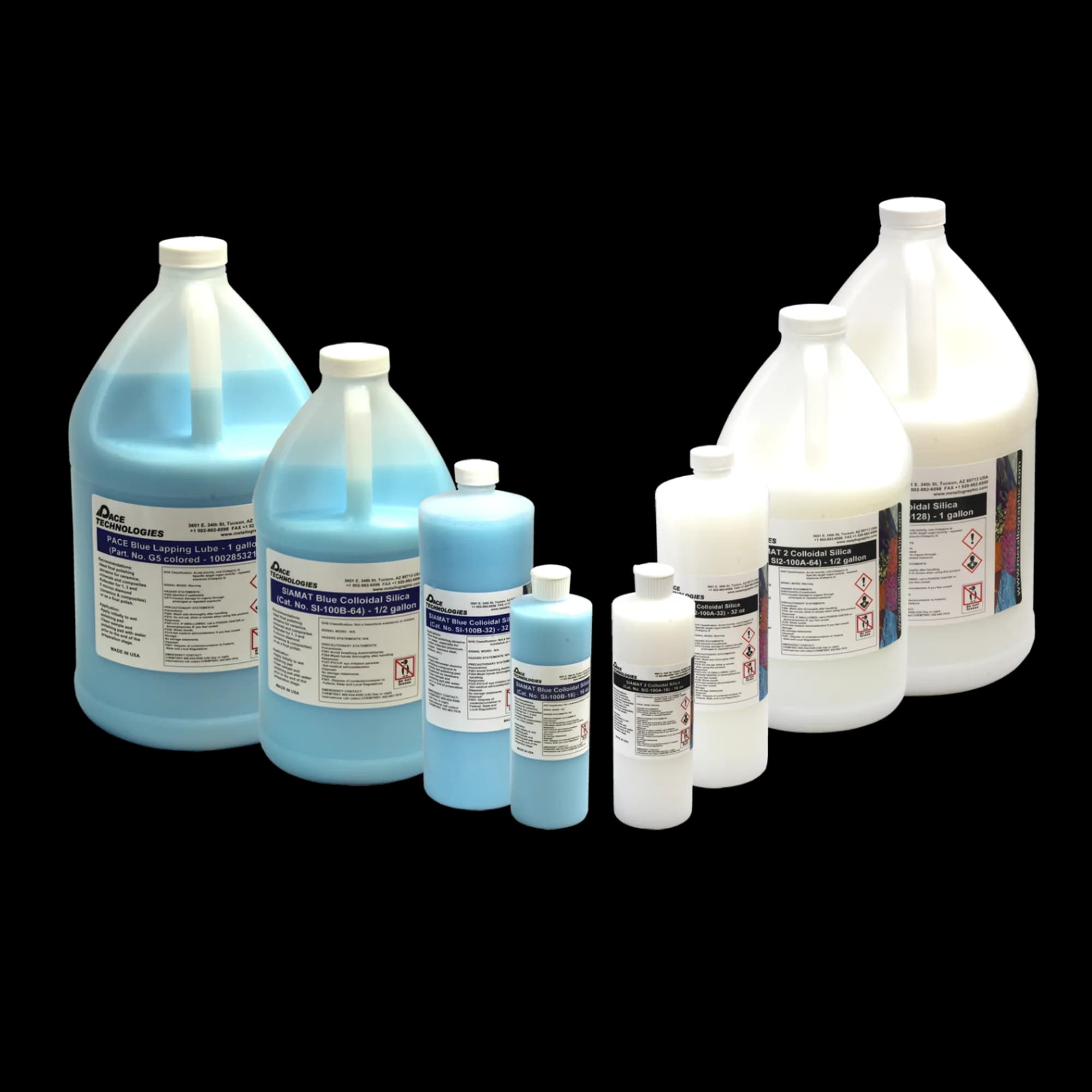
Colloidal silica for oxide polishing produces excellent surface finishes.
- 0.05 μm colloidal silica: 1-2 minutes on soft cloth
- Use light pressure to minimize material removal
- Rinse thoroughly with water
- Dry with compressed air (avoid touching the surface)
Polishing Considerations for PCBs and Chips
- Light Pressure: Always use minimal pressure to avoid delamination
- Short Times: Don't over-polish—just remove scratches from previous step
- Frequent Inspection: Check progress frequently under microscope
- Clean Between Steps: Thoroughly clean sample and change cloths between steps
- Material-Specific Rates: Be aware that different materials polish at different rates, which can create relief
- Solder Joints: Soft tin-based solders smear easily; a final polish of colloidal silica with a small ammonia addition helps lift smeared metal
Example Products: Polishing Pads and ClothsPolishing pads and cloths for different polishing stages
For purchasing options and product specifications, see commercial supplier website.
Specific Applications
Flip Chip Analysis
Flip chip packages require precise preparation to reveal bump structures, underfill, and interfaces. Controlled removal is essential to target specific bump rows or reveal the chip-to-substrate interface.
Computer chip cross-section showing flip chip structure. Proper preparation with controlled removal reveals bump structures, underfill, and layer interfaces critical for failure analysis.
Via and Through-Hole Analysis
Vias and through-holes are critical features in PCBs. Preparation must reveal:
- Via wall quality and plating thickness
- Via fill material (if present)
- Connection quality at layer interfaces
- Void detection in via structures
Solder Joint Analysis
Solder joints are prone to defects and require careful preparation to reveal:
- Intermetallic compound formation
- Void content and distribution
- Crack initiation and propagation
- Wetting quality
Layer Thickness Measurement
Precise layer thickness measurements require controlled removal to:
- Remove exact amounts of material
- Reveal layer interfaces clearly
- Maintain planarity for accurate measurements
- Prepare multiple samples consistently
Failure Analysis
Failure analysis often requires targeting specific failure sites:
- Precise depth control to reach failure location
- Minimal damage to preserve failure evidence
- Consistent preparation for comparison samples
- Preparation for SEM/FIB analysis
Troubleshooting Common Issues
Delamination
Symptoms: Layers separating, especially at interfaces
Solutions:
- Reduce polishing pressure
- Use shorter polishing times
- Ensure adequate mounting material penetration
- Consider vacuum impregnation during mounting
- Use controlled removal for more consistent results
Relief Between Materials
Symptoms: Height differences between copper, solder, and substrate
Solutions:
- Use controlled removal to maintain planarity
- Adjust polishing parameters for different materials
- Use appropriate polishing pads (harder pads for soft materials)
- Minimize final polish time to reduce relief
Smearing
Symptoms: Copper or solder smeared across surface
Solutions:
- Use harder polishing pads
- Reduce polishing pressure
- Use appropriate diamond size (not too fine too early)
- Ensure adequate lubrication
- Clean sample thoroughly between steps
Scratches
Symptoms: Visible scratches in final polish
Solutions:
- Ensure complete scratch removal at each grinding step
- Rotate sample 90° between grits
- Use fresh polishing compounds
- Clean polishing pads/cloths between uses
- Don't skip grit sizes in the grinding sequence
Over-Removal
Symptoms: Target feature removed or too much material removed
Solutions:
- Use controlled removal for precise depth control
- Monitor removal progress frequently
- Reduce polishing time
- Use lighter pressure
- Document parameters for future reference
Essential Equipment for PCB and Chip Preparation
Successful PCB and chip preparation requires specialized equipment, especially controlled removal systems, which provide the depth control and planarity that electronics cross-sections demand.