Microstructural Analysis
Learn how to prepare samples for microscopic examination, choose the appropriate microscope, and interpret microstructures to understand material properties and processing history.
Table of Contents
Introduction
Microstructural analysis is the final step in the metallographic process, where prepared samples are examined under a microscope to reveal their internal structure. This analysis provides critical information about material composition, processing history, and properties. Proper sample preparation and appropriate microscope selection are essential for obtaining meaningful results.

Example microstructure: Ferrite and pearlite in steel. Proper preparation and analysis reveal the internal structure that determines material properties.
This guide covers the complete process from final sample preparation through microscopic examination and interpretation. Understanding these steps ensures you can effectively analyze microstructures and extract meaningful information about your materials.
Preparing Samples for Microscopy
Before examining a sample under the microscope, it must be properly prepared. The quality of your preparation directly affects what you can see and how accurately you can interpret the microstructure. A poorly prepared sample can lead to incorrect conclusions about material structure and properties.
Final Preparation Steps
After grinding and polishing, several final steps ensure your sample is ready for microscopic examination:
- Thorough cleaning: Remove all polishing abrasives, debris, and contaminants. Use appropriate solvents (alcohol, acetone) and clean water. Dry completely with compressed air or lint-free cloth to prevent water spots or contamination.
- Surface inspection: Examine the sample surface under low magnification or with a hand lens to check for remaining scratches, contamination, or preparation artifacts. The surface should be mirror-like and free of visible defects.
- Etching (if required): Many materials require etching to reveal microstructure. Select the appropriate etchant for your material and apply according to standard procedures. See our Common Etchants Guide for material-specific recommendations.
- Post-etching cleaning: After etching, rinse thoroughly with appropriate solvents and dry completely. Some etchants leave residues that can interfere with examination.
- Storage: Store prepared samples in a clean, dry environment. Protect from dust, moisture, and physical damage. Consider using sample storage systems or protective covers.
Quality Checks Before Microscopy
Checklist for Sample Readiness
- ✓ Surface is mirror-like with no visible scratches
- ✓ Sample is clean and free of contamination
- ✓ Etching (if used) has revealed microstructure without over-etching
- ✓ Sample is dry and free of water spots or residues
- ✓ Sample is properly mounted and secure
- ✓ Sample orientation is correct for the analysis you need
Common Preparation Issues
Be aware of these common problems that can affect microscopic examination:
- Remaining scratches: Incomplete polishing leaves scratches that can be mistaken for microstructural features or obscure true structure
- Relief: Over-polishing creates height differences between phases, which can affect focus and interpretation
- Contamination: Embedded abrasives, polishing compounds, or other contaminants can appear as microstructural features
- Over-etching: Excessive etching can obscure fine details or create artifacts
- Under-etching: Insufficient etching may not reveal the microstructure adequately
- Edge rounding: Poor edge retention can make edge analysis difficult or impossible
Tip: If you're unsure about sample quality, examine it under low magnification first. Many preparation issues are visible at 50-100x and can be corrected before detailed analysis. A well-prepared sample makes all subsequent analysis much easier and more accurate.
Choosing the Right Microscope
Selecting the appropriate microscope depends on your analysis requirements, material type, and available resources. Different microscopes offer different capabilities, and understanding these helps you make the right choice for your needs.
Metallurgical (Optical) Microscopes
Metallurgical microscopes use reflected light to examine opaque samples. They are the standard choice for most routine metallographic analysis:
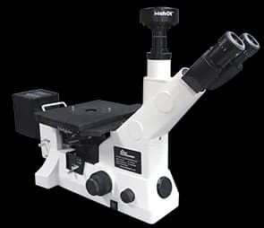
Metallurgical microscopes are the standard tool for routine microstructural analysis, offering magnifications from 50x to 1000x with various illumination modes.
- Magnification range: Typically 50x to 1000x (up to 2000x with oil immersion)
- Best for: Routine analysis, grain size measurement, phase identification, quality control
- Advantages: Relatively affordable, easy to use, fast analysis, good for most materials
- Limitations: Limited resolution (~0.2-0.3 μm), lower magnification than SEM
Scanning Electron Microscopes (SEM)
SEM provides much higher magnification and resolution than optical microscopes:
- Magnification range: Up to 100,000x or more
- Best for: High-magnification analysis, fracture surfaces, fine features, elemental analysis (with EDS)
- Advantages: High resolution, excellent depth of field, can analyze chemistry
- Limitations: More expensive, requires more sample preparation, slower analysis
Stereo Microscopes
Stereo microscopes provide 3D viewing at low magnifications:
- Magnification range: Typically 5x to 50x
- Best for: Sample inspection, fracture surface examination, general observation
- Advantages: 3D viewing, easy to use, good for initial sample assessment
- Limitations: Low magnification, not suitable for detailed microstructural analysis
Decision Guide
Which Microscope Should You Use?
Routine analysis, grain size, phase identification?
→ Use Metallurgical Microscope
Need very high magnification or examining fracture surfaces?
→ Use SEM
Initial sample inspection or general observation?
→ Use Stereo Microscope
Need elemental analysis or chemical information?
→ Use SEM with EDS
Microscopy Methods and Techniques
Different microscopy techniques reveal different aspects of microstructure. Understanding these methods helps you select the appropriate technique for your analysis needs and interpret what you observe.
Optical Microscopy Techniques
Optical (light) microscopy is the most common and accessible technique for metallographic examination. Standard metallurgical microscopes use reflected light illumination, allowing observation of opaque samples. Various illumination modes provide different information:
Brightfield Illumination
The standard illumination mode. Light reflects from the sample surface, with different phases appearing with different brightness based on their reflectivity and etching response. Most common for routine metallographic examination.
Darkfield Illumination
Uses oblique illumination to highlight surface features. Reveals details like scratches, porosity, and inclusions that may be less visible in brightfield. Useful for examining as-polished surfaces and detecting preparation artifacts.
Polarized Light
Uses polarized light to reveal crystallographic features. Particularly useful for non-cubic materials (titanium, zirconium, some ceramics) and for examining anisotropic features. Can reveal grain orientation differences.
Differential Interference Contrast (DIC)
Enhances contrast by converting height differences into color differences. Excellent for revealing relief (height differences between phases) and fine surface details. Particularly useful for examining polished surfaces and detecting subtle microstructural features.
Typical Magnification Range: 50x to 1000x (occasionally up to 2000x with oil immersion). Most routine analysis is performed at 100x to 500x.
Scanning Electron Microscopy (SEM)
SEM uses a focused electron beam to scan the sample surface, providing much higher magnification and resolution than optical microscopy:
- Higher magnification: Up to 100,000x or more, compared to ~1000x for optical microscopy
- Greater depth of field: More of the sample appears in focus, especially useful for rough surfaces like fracture surfaces
- Fracture surface examination: Ideal for failure analysis, as fracture surfaces don't require polishing
- Elemental analysis: Can be equipped with EDS (energy-dispersive X-ray spectroscopy) for chemical analysis
.JPG&w=1080&q=75)
SEM image at 20,000x magnification showing fine microstructural details not visible with optical microscopy.
Advanced Techniques
Electron Backscatter Diffraction (EBSD)
Provides crystallographic information including grain orientation, texture, and phase identification. Creates orientation maps showing how grains are oriented relative to each other. Essential for understanding deformation, recrystallization, and texture development.
Energy-Dispersive X-ray Spectroscopy (EDS)
Chemical analysis technique that identifies elements present in the microstructure. Can be used with SEM or TEM. Provides elemental composition maps and point analyses. Essential for identifying phases, inclusions, and understanding chemical segregation.
Focused Ion Beam (FIB)
Uses a focused ion beam to precisely section specific regions of interest. Allows preparation of TEM samples from exact locations. Can also be used for in-situ sectioning and observation. Particularly valuable for failure analysis and examining specific features.
Transmission Electron Microscopy (TEM)
Very high magnification (up to millions of times) for atomic-scale analysis. Requires extremely thin samples (typically less than 100 nm). Used for examining dislocations, fine precipitates, interfaces, and nanoscale features. Advanced research technique.
Choosing the Right Technique: Start with optical microscopy for most routine analysis. Use SEM for higher magnification needs, fracture surfaces, or when elemental analysis is required. Advanced techniques like EBSD and TEM are specialized tools for specific research questions.
Common Microstructures and What They Mean
Learning to recognize common microstructures helps you understand what you're seeing and what it means for material properties. This section provides examples of typical microstructures in different materials, along with explanations of what they indicate about processing history and properties.
Steel Microstructures
Ferrite-Pearlite Steel

What you see: Light regions are ferrite (soft, ductile phase). Dark regions with lamellar structure are pearlite (alternating ferrite and cementite plates).
What it means: Slow cooling from austenite (annealing or furnace cooling). Moderate strength, good ductility, machinable. Typical of normalized or annealed low-carbon steels.
Properties: Balanced strength and ductility. Good for general engineering applications.
Pearlite

What you see: Alternating light and dark lamellae (plates). The spacing depends on cooling rate: faster cooling produces finer pearlite.
What it means: Eutectoid transformation from austenite. Fine pearlite (from faster cooling) is stronger than coarse pearlite.
Properties: Moderate strength, good machinability. Finer pearlite has higher strength and hardness.
Stainless Steel

What you see: Martensitic structure with fine, needle-like or lath features. May show prior austenite grain boundaries.
What it means: Quenched and tempered martensitic stainless steel. High strength and hardness with good corrosion resistance.
Properties: High strength, good wear resistance, moderate toughness. Used in applications requiring strength and corrosion resistance.
Cast Iron Microstructures
Gray Cast Iron

What you see: Graphite flakes (dark, irregular shapes) in a matrix of ferrite and/or pearlite.
What it means: Slow cooling allows graphite to form as flakes. The matrix structure depends on cooling rate and composition.
Properties: Good machinability, excellent damping capacity, but brittle. Graphite flakes act as stress concentrators.
Nodular (Ductile) Cast Iron
.JPG&w=828&q=75)
What you see: Spherical or nodular graphite particles (dark circles) in a ferrite or pearlite matrix.
What it means: Magnesium or cerium treatment causes graphite to form as spheres instead of flakes. Much stronger and more ductile than gray iron.
Properties: Good strength and ductility (hence "ductile iron"). Better mechanical properties than gray iron while maintaining castability.
Aluminum Alloy Microstructures
Aluminum-Silicon Alloy

What you see: Silicon particles (dark) in an aluminum matrix. May show precipitates, grain boundaries, and eutectic structure.
What it means: Cast or heat-treated aluminum alloy. Silicon improves castability and can form strengthening precipitates.
Properties: Lightweight, good castability, moderate strength. Common in automotive and aerospace applications.
Copper Alloy Microstructures
Copper (Tough Pitch)

What you see: Equiaxed grains with annealing twins (straight lines within grains). May show oxide particles.
What it means: Annealed copper with recrystallized grain structure. Twins indicate low stacking fault energy and annealing.
Properties: Excellent electrical and thermal conductivity, good ductility, corrosion resistance.
Brass (70-30)

What you see: Elongated grains showing directionality from rolling. May show annealing twins.
What it means: Cold-worked or partially recrystallized brass. Elongated grains indicate mechanical working.
Properties: Good strength and formability. Elongated structure indicates work hardening from rolling.
Titanium Alloy Microstructures
Titanium with ZrB₂
.JPG&w=828&q=75)
What you see: Alpha/beta titanium structure with reinforcing particles. May show Widmanstätten structure or equiaxed grains.
What it means: Titanium matrix composite or alloy. The structure depends on heat treatment and processing.
Properties: High strength-to-weight ratio, excellent corrosion resistance. Used in aerospace and medical applications.
Learning to Interpret Microstructures: Start by identifying the phases present, then consider grain size and distribution, and finally relate these to processing history and properties. With practice, you'll develop the ability to quickly assess material condition and processing from microstructure examination.
Microstructural Interpretation
Interpreting microstructures involves understanding what you observe and relating it to material properties and processing history. This requires knowledge of phase transformations, processing effects, and material behavior.
Systematic Approach to Interpretation
- Identify phases present: What phases can you see? Are they expected for this material and composition?
- Assess grain size: Is the grain size fine, medium, or coarse? How does this relate to processing?
- Examine phase distribution: Are phases uniformly distributed or segregated? Are there clusters or bands?
- Look for processing indicators: Elongated grains suggest mechanical working. Fine structures suggest rapid cooling. Coarse structures suggest slow cooling or high temperatures.
- Check for defects: Are there inclusions, porosity, cracks, or other defects?
- Relate to properties: How does the observed structure relate to expected material properties?
Quantitative Microstructural Measurements
When the analysis requires numbers rather than descriptions, use the established standard methods:
- Grain size: ASTM E112 (comparison-chart, intercept, and planimetric methods); ASTM E1382 for grain size by semiautomatic or automatic image analysis
- Inclusion content of steel: ASTM E45 (worst-field method with reference charts)
- Phase (volume) fraction: ASTM E562 (systematic point counting, manual or automated)
All of these methods assume a deformation-free surface with a uniform etch — residual scratches, smearing, relief, or uneven grain-boundary etching bias the measurement before any counting begins. If the preparation is questionable, fix it before quantifying anything.
Common Interpretation Challenges
- Preparation artifacts: Scratches, contamination, or relief can be mistaken for microstructural features
- Etching effects: Over-etching or under-etching can obscure or create false features
- Magnification effects: Features may look different at different magnifications
- Sample orientation: The same structure can look different depending on the plane of section
- Phase identification: Some phases look similar and require additional analysis (e.g., EDS) for positive identification
Best Practice: When in doubt, examine the sample at multiple magnifications and compare with reference microstructures. Document your observations with photomicrographs for future reference and comparison.